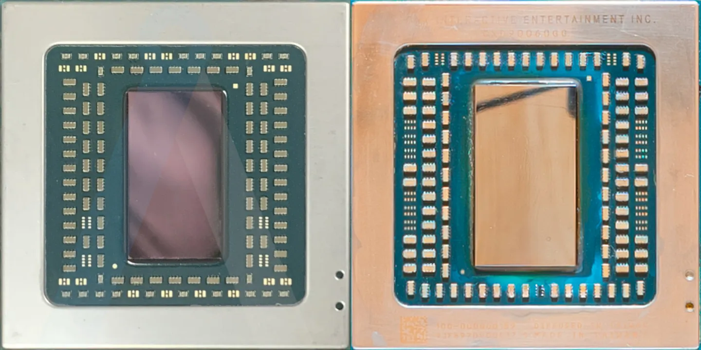
In the last month, Sony has begun the rollout of their latest revision of the PlayStation 5, model CFI-1202. There has already been a teardown showing the model’s redesigned board and cooling that is smaller and lighter. Power consumption is also reduced while giving the similar performance. To accomplish this, AMD’s Semi-Custom design teams have ported the PS5 silicon to TSMC N6, codename Oberon Plus. Angstronomics reveals exclusive images of the new, smaller die, and we discuss the how and the why behind this update.

6nm Oberon Plus vs 7nm Oberon
With an exclusive side-by-side comparison showing 6nm Oberon Plus next to 7nm Oberon, we can see what has physically changed in the 2 years between them. Die size has gone from ~300 mm² to below 260 mm², a shrink of close to 15%. What this means in the end is that each wafer processed can produce near 20% more chips for a similar cost.


